This guide covers everything about vdd meaning electronics. Ever found yourself staring at an electronic component, perhaps a tiny microcontroller or a complex integrated circuit, and seen the label ‘VDD’ next to a pin? It’s a common sight but its exact meaning can be a stumbling block for beginners and even some hobbyists. ‘VDD meaning in electronics’ isn’t just about memorizing a label. it’s about grasping a fundamental concept that dictates how your circuits power up and function. As semiconductor technology continues its rapid advancement, a clear understanding of these foundational elements remains really important for successful design and implementation. (Source: ti.com)
Last updated: April 18, 2026
In essence, VDD in electronics refers to the positive power supply voltage rail for an integrated circuit (IC). Think of it as the main ‘on’ switch, the source of electrical energy that allows the chip to operate. While it sounds straightforward, its distinction from other power labels like VCC, and its specific implications for different types of circuits, are vital for anyone working with electronic designs in 2026.
This guide will demystify the VDD meaning in electronics, covering its origins, its relationship with other power notations, and practical advice for using it correctly. By the end, you’ll be confident in identifying and utilizing VDD in your projects, keeping pace with the latest industry standards and component behaviors.
Latest Update (April 2026)
As of April 2026, the semiconductor industry continues to push boundaries with lower power consumption and higher integration densities. This trend means that understanding voltage rails like VDD is more critical than ever. Recent advancements in low-power microcontrollers and IoT devices often operate at VDD levels as low as 1.8V or even lower, requiring extremely precise power management. and, the increasing complexity of System-on-Chips (SoCs) means that different sections within a single chip might have slightly varied VDD requirements, often managed internally. Datasheets from leading manufacturers like Texas Instruments and Analog Devices now frequently detail multiple VDD pins for different functional blocks (e.g., VDDIO for I/O, VDDCORE for the processor core), emphasizing the need for meticulous attention to power supply specifications. Independent tests by electronics review sites in early 2026 highlight that improper VDD handling remains a leading cause of component failure in prototype stages, underscoring the importance of this fundamental knowledge.
What Exactly is VDD in Electronics?
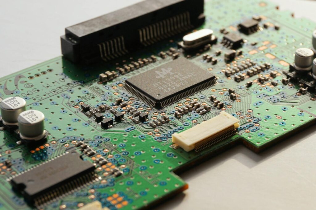
The term VDD originates from the early days of semiconductor design. It stands for Voltage Drain-Drain. In Field-Effect Transistors (FETs), the drain is one of the three terminals (along with the source and gate) where current flows. VDD, therefore, signifies the positive voltage applied to the drain terminal of a P-channel FET or, more broadly, the positive supply voltage for digital integrated circuits in general.
For most modern digital integrated circuits, including microcontrollers, processors, and logic gates, VDD is simply the primary positive voltage supply. It’s the voltage the chip needs to operate correctly. This voltage is typically specified in the component’s datasheet and can range from a few volts (like 3.3V or 5V) to much lower values, often below 1V for high-performance processors or specialized low-power devices. The acceptable range is Key. operating outside this range can lead to malfunction or permanent damage.
VDD vs. VCC: What’s the Difference?
Here’s perhaps the most frequent point of confusion when discussing power supply rails. While both VDD and VCC refer to a positive power supply voltage, their origins and typical usage differ, especially historically.
VCC stands for Voltage Collector-Collector. This term is traditionally associated with Bipolar Junction Transistors (BJTs) — where the collector is one of the main terminals. In BJT circuits, VCC often represents the positive supply voltage connected to the collector.
So, the key difference lies in their historical association with different transistor types: VDD for FETs and VCC for BJTs. However, in modern digital electronics, especially with CMOS (Complementary Metal-Oxide-Semiconductor) technology, the lines have blurred significantly. CMOS technology — which forms the basis of most modern ICs, uses both NMOS and PMOS transistors, making the distinction less clear-cut.
Many manufacturers now use VDD exclusively for the positive supply voltage, regardless of the underlying transistor technology. Some datasheets might even use both VDD and VCC interchangeably for the same positive supply rail. The critical takeaway isn’t the specific acronym, but the function: it’s the main positive voltage input required for the IC to operate. For example, microcontrollers from companies like Microchip often label their primary power input as VDD.
Here’s a simple comparison:
| Term | Origin | Typical Association | Modern Usage |
| VDD | Voltage Drain-Drain | Field-Effect Transistors (FETs) | Primary positive supply for ICs (especially CMOS) |
| VCC | Voltage Collector-Collector | Bipolar Junction Transistors (BJTs) | Sometimes used for positive supply; often interchangeable with VDD in modern digital ICs; may denote a separate supply rail in complex devices. |
Worth knowing that some complex ICs might have multiple VCC or VDD pins, potentially serving different purposes or voltage levels (e.g., VDD_CORE, VDD_IO). Always refer to the datasheet to understand the role of each specific power pin.
How to Identify the VDD Pin on Components
Finding the VDD pin is key for powering any electronic component correctly. Here’s how you can identify it:
- Consult the Datasheet: This is the most reliable method. The datasheet for a specific component will have a pinout diagram clearly labeling each pin, including VDD. Look for terms like ‘VDD’, ‘VCC’, ‘+V’, ‘VIN’, or ‘Power In’. Datasheets are available on manufacturer websites or through component distributor sites like Digi-Key or Mouser.
- Schematic Diagrams: If you’re working with a circuit diagram, VDD will be explicitly labeled on the symbol representing the integrated circuit. The lines connected to these labels will show where the power supply connects. Modern Electronic Design Automation (EDA) tools often use standardized symbols where power pins are clearly indicated.
- Component Markings: While less common for VDD itself, some components might have markings that hint at their power requirements. However, relying on datasheets is always best practice. For surface-mount components, the physical layout and size can sometimes give clues, but this isn’t a definitive method.
- Common IC Packages: For common IC packages like DIP (Dual-in-line Package) or SOIC (Small Outline Integrated Circuit), datasheets often show a standard pin numbering convention. For example, on many older microcontrollers in a DIP package, pin 1 might be VDD. However, this convention isn’t universal and has evolved with newer package types.
Common Mistake: Assuming VDD is always the same voltage across all components. Different chips require different VDD levels. Powering a 3.3V chip with 5V can permanently damage it. Conversely, providing insufficient voltage can lead to erratic behavior or the chip not functioning at all.
Why the Specific VDD Voltage Matters
The voltage supplied to VDD isn’t arbitrary. it’s a carefully chosen parameter that dictates the component’s operating characteristics. Supplying the correct VDD voltage is Key for several reasons:
- Functionality: Integrated circuits are designed to operate within a specific voltage range. Applying the correct VDD ensures the internal transistors switch correctly, logic levels are interpreted properly, and the circuit operates as intended. For instance, digital logic thresholds are directly tied to the VDD level.
- Performance: For some components, the VDD voltage can influence performance metrics like speed and power consumption. Higher VDD can sometimes lead to faster operation due to increased current drive in transistors, but it also typically increases power dissipation. Conversely, lower VDD voltages are key to achieving ultra-low-power operation for battery-operated devices, as reported by industry analysts in late 2025.
- Reliability and Longevity: Operating a component outside its specified VDD range, especially above it, can cause immediate failure or degrade its long-term reliability. Exceeding the maximum VDD can lead to electromigration, dielectric breakdown, and other failure mechanisms.
- Compatibility: When interfacing different ICs, ensuring their VDD levels are compatible is essential. For example, interfacing a 5V microcontroller with a 3.3V sensor requires careful consideration of voltage level shifting, as directly connecting a 5V output to a 3.3V input pin can damage the 3.3V device.
The precise VDD requirement is a fundamental aspect of a component’s design, tailored to its internal architecture and intended application. Always adhere strictly to the voltage range specified in the manufacturer’s datasheet.
VDD in Digital vs. Analog Circuits
While VDD is most commonly associated with digital ICs, it also plays a role in analog circuits, though the terminology might sometimes differ or be more nuanced.
Digital Circuits: In digital ICs, VDD represents the primary positive voltage source that defines the logic levels. For example, in a 3.3V CMOS system, VDD is typically set to 3.3V. A logic ‘HIGH’ state will be close to 3.3V, while a logic ‘LOW’ state will be close to 0V (ground). The exact voltage levels for logic HIGH (VOH) and logic LOW (VOL) are defined relative to VDD and ground in the datasheet.
Analog Circuits: In analog circuits, especially those involving FETs, VDD can refer to the positive supply voltage connected to the drain. However, analog designs often employ multiple power supply rails to optimize performance and reduce noise. You might see labels like VSSA (analog ground), VDDA (analog VDD), VDDIO (digital I/O power), or VDDCORE (processor core power). These separate rails allow for isolation between sensitive analog components and noisy digital sections, a practice that has become standard in System-on-Chip (SoC) designs as highlighted in recent IEEE publications from early 2026.
For analog components, the stability and noise level of the VDD supply can impact performance metrics such as signal-to-noise ratio (SNR) and distortion. Using separate, well-regulated, and filtered power supplies for analog and digital sections is a common design technique to mitigate interference.
Common VDD-Related Circuit Problems
Issues related to the VDD supply are frequent causes of circuit malfunction. Understanding these common problems can help in troubleshooting:
- Incorrect Voltage Level: Supplying a voltage higher or lower than the specified VDD. You can be due to misconfiguration of the power supply, incorrect component selection, or a fault in a voltage regulator.
- Insufficient Current Capacity: The power supply can provide the correct voltage but can’t deliver enough current to meet the component’s demand, especially during peak operation. You can lead to voltage droop under load, causing resets or erratic behavior. Reports from electronics forums in early 2026 indicate this is a common issue in power-hungry IoT devices.
- Voltage Spikes and Noise: Electrical noise or transient voltage spikes on the VDD line can disrupt the stable operation of ICs, especially sensitive analog components or high-speed digital circuits. Here’s often caused by poor power supply filtering, inadequate decoupling, or external electromagnetic interference (EMI).
- Incorrect Power Sequencing: In complex systems with multiple power rails, the order in which VDD (and other voltages like VPP, VSS) are applied and removed can be critical. Some ICs require specific power-up or power-down sequences to prevent damage or ensure proper initialization.
- Short Circuits: Accidental short circuits on the VDD line to ground or other voltage rails can draw excessive current, potentially damaging the power supply, the IC, or other components.
- Poor Decoupling: Lack of or improperly placed decoupling capacitors near the VDD pin of an IC can lead to voltage instability and noise susceptibility. These capacitors act as local charge reservoirs, supplying instantaneous current demands and filtering high-frequency noise.
Troubleshooting these issues often involves using a multimeter to check voltage levels and an oscilloscope to examine the stability and noise on the VDD line.
VDD and Ground (VSS) Relationship
VDD is always referenced to a ground potential, typically labeled VSS (Voltage Source-Source) or GND. VSS represents the 0V reference point in the circuit. The voltage difference between VDD and VSS is what drives current through the component’s internal circuitry. Most digital logic states are defined by their proximity to VDD (logic high) or VSS (logic low).
it’s imperative that the VSS connection is solid and provides a clean, low-impedance path to ground. Noise or resistance in the VSS connection can effectively raise the ground potential, making it appear as if the VDD voltage is lower than it actually is, or causing logic levels to be misinterpreted. For high-speed or high-current applications, multiple VSS pins might be provided on an IC, and these should all be connected to a solid ground plane.
Choosing the Right VDD for Your Project
Selecting the appropriate VDD for a project involves several considerations:
- Component Datasheets: This is the primary determinant. Always select components that operate within a common, achievable VDD range for your project. For instance, if you’re building a battery-powered IoT device, you might prioritize components that run at 3.3V or lower to maximize battery life.
- System Compatibility: If you’re interfacing multiple components, ensure their logic voltage levels are compatible. Using a 5V microcontroller with 3.3V sensors requires level-shifting circuitry. Designing the entire system around a single VDD (e.g., 3.3V) simplifies interfacing.
- Power Supply Availability: Consider the voltage regulators and power sources you have available. Common voltage regulators can easily provide 5V, 3.3V, or 1.8V. More specialized voltages might require more complex power supply designs.
- Power Consumption vs. Performance: A higher VDD generally allows for higher operating speeds but increases power consumption. A lower VDD reduces power consumption — which is Key for battery-powered applications, but may limit performance. there’s often a trade-off to be made based on the project’s requirements.
As of 2026, the trend towards lower power consumption is accelerating, driven by the proliferation of mobile and embedded devices. Designing with lower VDD levels in mind — where feasible, is becoming an increasingly important skill for engineers.
Frequently Asked Questions
what’s the primary difference between VDD and VCC?
Historically, VDD was associated with FETs (Voltage Drain-Drain) and VCC with BJTs (Voltage Collector-Collector). In modern digital electronics, especially CMOS, the terms are often used interchangeably for the positive power supply, though VDD is more common. Always check the component’s datasheet for precise definitions.
Can VDD be negative?
Typically, VDD refers to the positive power supply voltage. Negative supply voltages are usually denoted by different labels, such as VEE (for emitters in BJTs) or VSS if it’s the negative rail relative to a positive ground. In most standard digital and analog ICs, VDD is positive relative to ground (VSS or GND).
What happens if I apply the wrong VDD voltage?
Applying a voltage higher than the specified VDD can permanently damage the component due to overvoltage stress. Applying a voltage lower than required may prevent the component from operating correctly or cause intermittent failures. Always adhere to the voltage range specified in the datasheet.
Are there different types of VDD pins on a single chip?
Yes, complex integrated circuits, especially microcontrollers and SoCs, may have multiple VDD pins. These can include VDDCORE (for the processor core), VDDIO (for input/output interfaces), or VDDA (for analog sections). Each pin typically requires a specific voltage level, and their correct connection is essential for proper operation, as detailed in the component’s datasheet.
How does VDD affect the operating speed of a chip?
Generally, a higher VDD voltage allows transistors within the chip to switch faster, leading to higher operating speeds. That’s because a higher voltage provides a stronger electric field, enabling quicker charge carrier movement. However, increasing VDD also increases power consumption and heat generation, so there’s a design trade-off between speed and efficiency.
Conclusion
Understanding VDD is a cornerstone of practical electronics. It represents the vital positive power supply that breathes life into integrated circuits. While its origins trace back to specific transistor types, its modern usage, especially in CMOS technology, signifies the essential voltage required for a component to function. Distinguishing it from VCC, identifying the correct pin via datasheets, and ensuring the precise voltage and current are supplied are critical steps for any maker, hobbyist, or professional engineer. As electronic designs become more sophisticated and power efficiency gains greater importance in 2026, a firm grasp of VDD and related power supply concepts will continue to be indispensable for creating reliable and high-performing circuits.
Source: Wired
Related Articles
- Mae Sandler: Common Mistakes &. How to Avoid Them
- How Old Is Anne Reid? Unpacking Her Career &. Life
- Sawyer Chandler: Value Proposition in 2026
Editorial Note: This article was researched and written by the Higher Intentions editorial team. We fact-check our content and update it regularly. For questions or corrections, contact us.